Needham Laser Tech logo

Electronics

Marking with precision and accuracy

Made in Britain logo

Electronics & PCB Laser Etching Machine

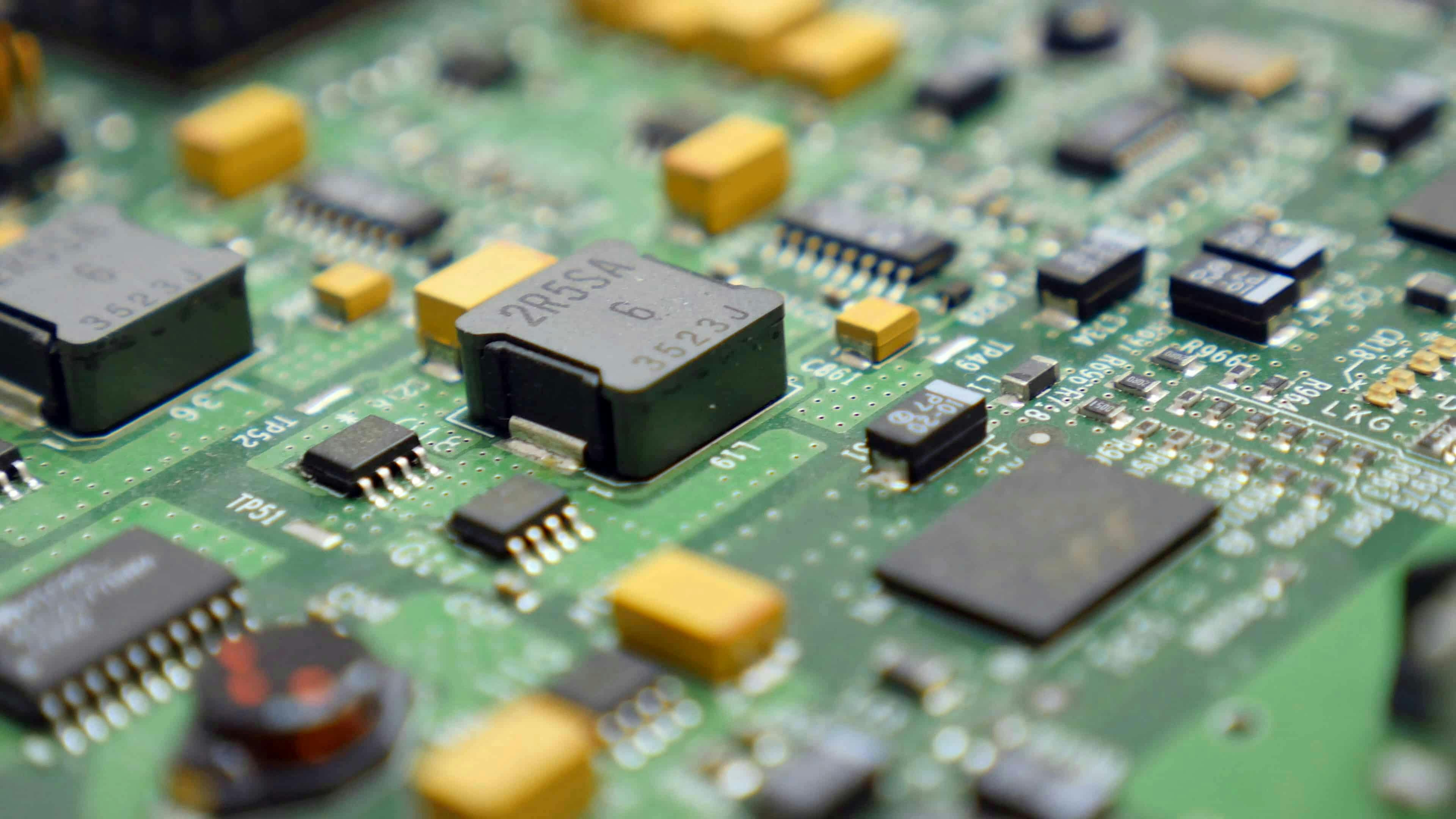
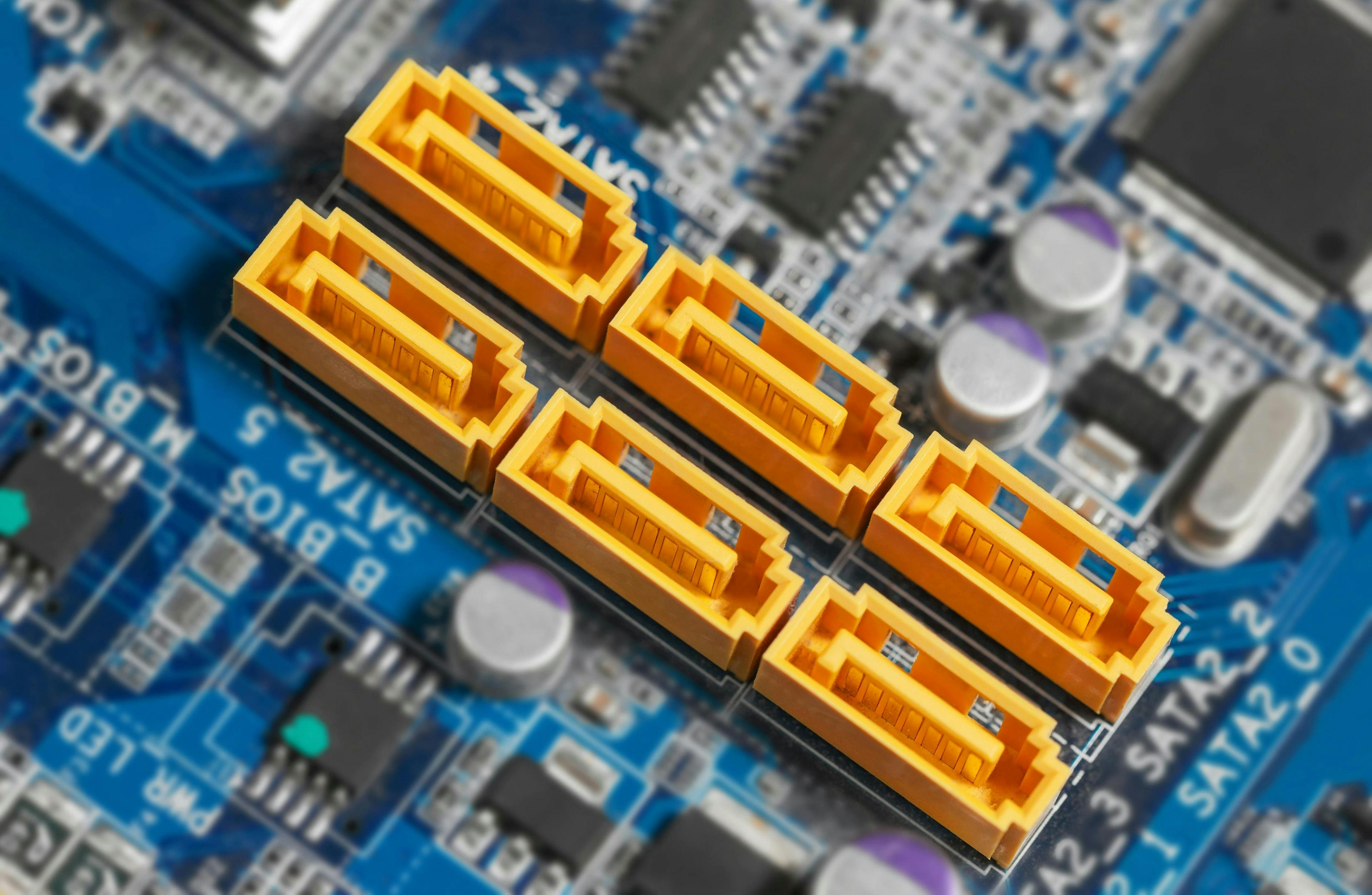
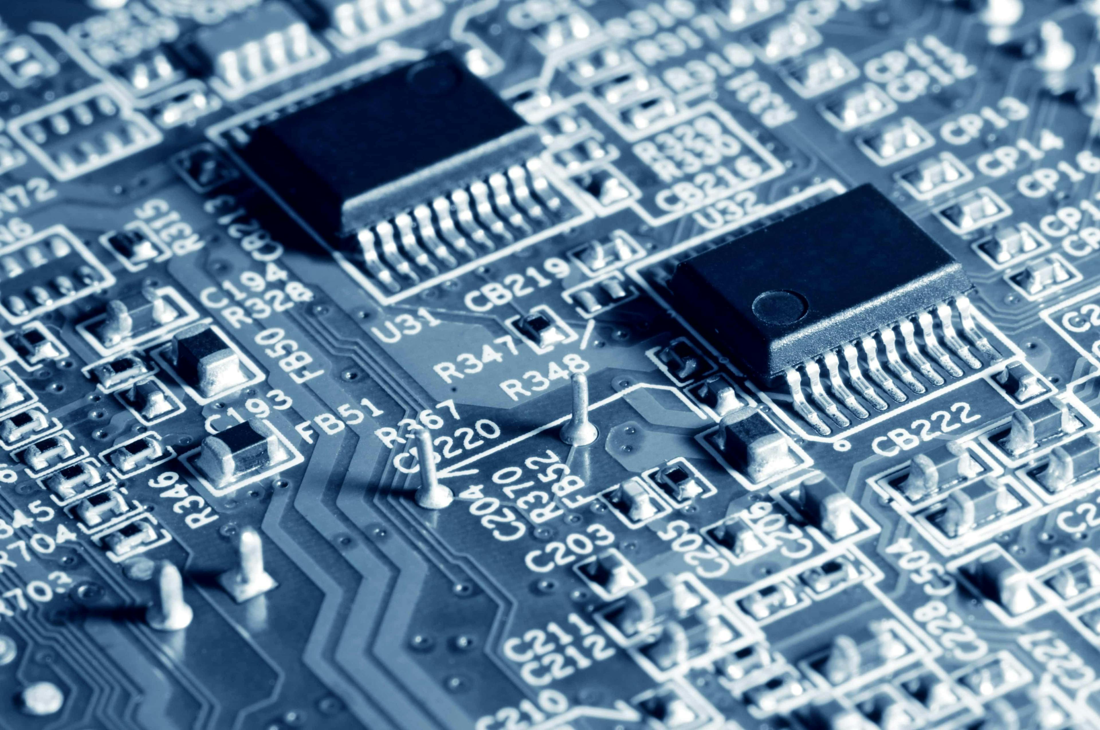
In the manufacturing of electronics, laser etching has been used to create customised process control boards (PCBs).

PCBs are the brains behind most consumer electronics, providing a compact system for the controlled connection of different electronic components. A laser etching machine for PCB allows custom PCBs to be manufactured rapidly and with pinpoint accuracy. In terms of speed, accuracy and cost, laser etching trumps all other methods of PCB manufacturing.

Aside from executing PCB designs, a PCB engraving laser can also be used to mark various electrical components with critical information such as barcodes, part numbers, 2D and UID codes, QR codes, serial numbers, batch numbers, logos, and business information. These marks allow manufacturers to improve traceability, identify specific electrical components during warranty claims, enforce trademark protection and more.

To learn more about how our electronics and PCB coding and marking equipment can have substantial benefits for your business, call Needham Laser Tech at 01948 660011 or fill out our online contact form to get a call back.

The Demands of the Electronics Industry

Aside from executing PCB designs, a laser marking machine for PCB can also be used to mark various electrical components with critical information such as barcodes, part numbers, 2D and UID codes, QR codes, serial numbers, batch numbers, logos, and business information. These marks allow manufacturers to improve traceability, identify specific electrical components during warranty claims, enforce trademark protection, and more.

Laser etching is used to mark semiconductors, circuit breaker parts, metal and plastic housings, and other surface-mount devices (SMDs). These electrical components are practically everywhere - from your smartphone to the circuit breaker in your basement, the electronics in your car, and even the satellites orbiting in outer space. Laser marking of electronic components delivers benefits for projects of all sizes and can be adapted into all manufacturing lines.

Laser marking can be used to mark most industrial materials such as marble, ceramic, granite, and several metals. Metal etching is commonly accomplished by applying a thin layer of paint to the metal surface first, which the laser vaporises during the etching process.

The N-Lase Range

Meet our Industrial ID lasers

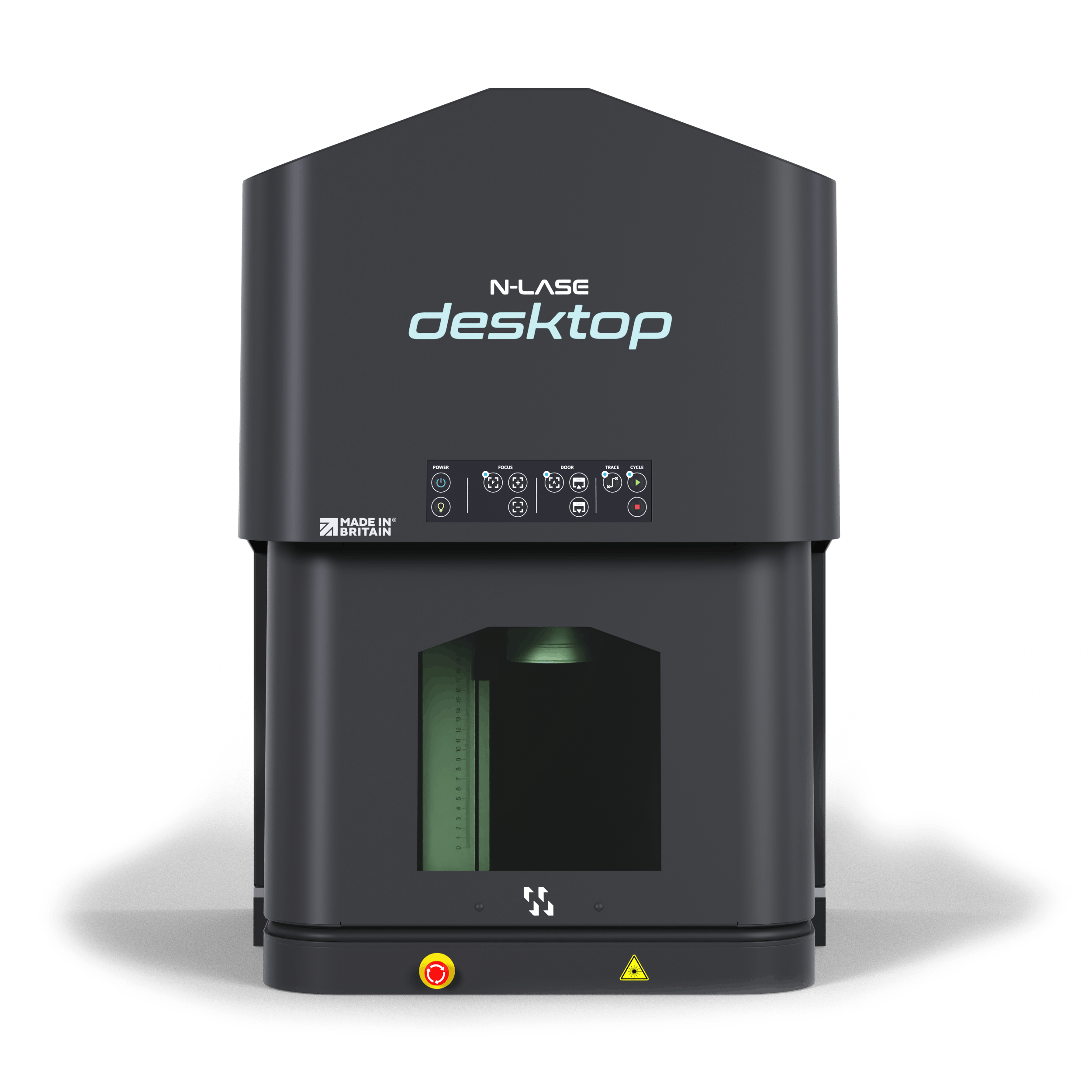
N-Lase Desktop

The N-Lase Desktop is our entry-level laser marking system for industrial identification applications, perfect for marking, etching, engraving and annealing all metals, coated metals, plastics and some organic materials.

The Desktop is the ideal solution for low to mid-volume throughput and is an affordable alternative to more traditional methods of marking, such as dot peen, electrochemical etching or hand marking. Despite being entry-level and affordable we haven’t sacrificed on quality or efficiency; our N-Lase Desktop comes with either our 20 Watt or 50 Watt MOPA fiber laser with a MTBF of 100,000 marking hours and a 3-year comprehensive warranty, as standard.

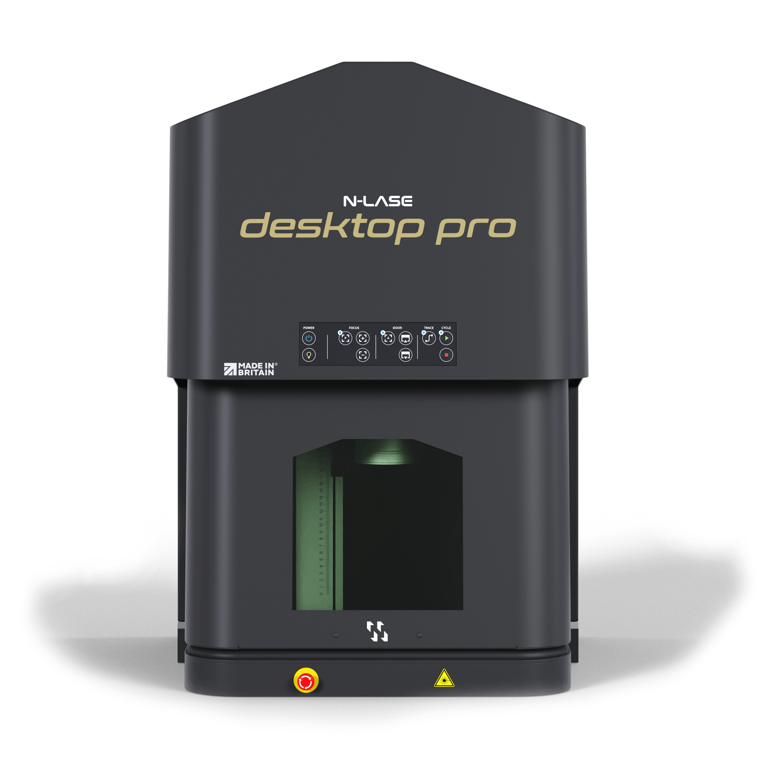
N-Lase Desktop Pro

The N-Lase Desktop Pro is the most popular laser in our N-Lase range. Designed for marking, etching, engraving and annealing almost all materials in mid to high-volume applications, the Desktop Pro is a full turnkey solution which includes an integrated All-in-One PC and an automatic door function to ensure maximum efficiency and simple operation.

The N-Lase Desktop Pro can be fitted with either our 20 Watt or 50 Watt MOPA fiber laser sources with a MTBF of 100,000 marking hours. Like all products within our N-Lase range the Desktop Pro comes with a 3-year comprehensive warranty, as standard.

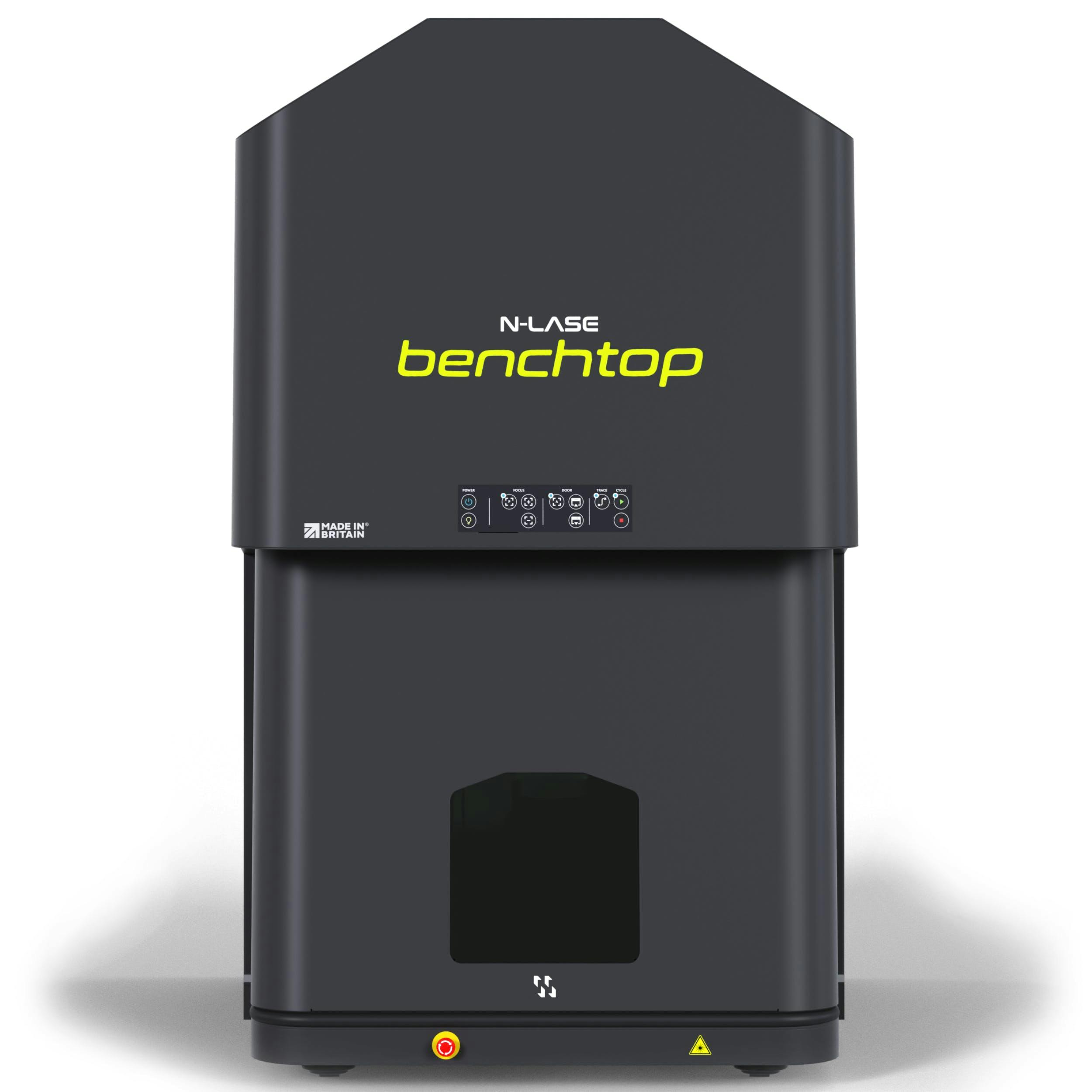
N-Lase Benchtop

The N-Lase Benchtop is the ‘big cousin’ to the Desktop Pro. It has the same style and design but on a much larger scale, so maximum versatility for industries wishing to mark, etch and engrave big parts. As the name suggested, the Benchtop is designed to sit on a bench/worktop within existing manufacturing cells and processes.

Due to its larger footprint and modular design, the N-Lase Benchtop can offer a broad range of optional extras such as XY marking tables for increased throughput, large marking area lenses (up to 280mm x 280mm), big rotary attachments for circumference marking on large diameter parts and power sources from 20 watt up to 100 watt for maximum speed and depth.

With our 3-year comprehensive warranty, the N-Lase Benchtop is the ideal solution for the efficient and reliable etching of heavy-duty parts in industrial environments.

N-Lase Workstation

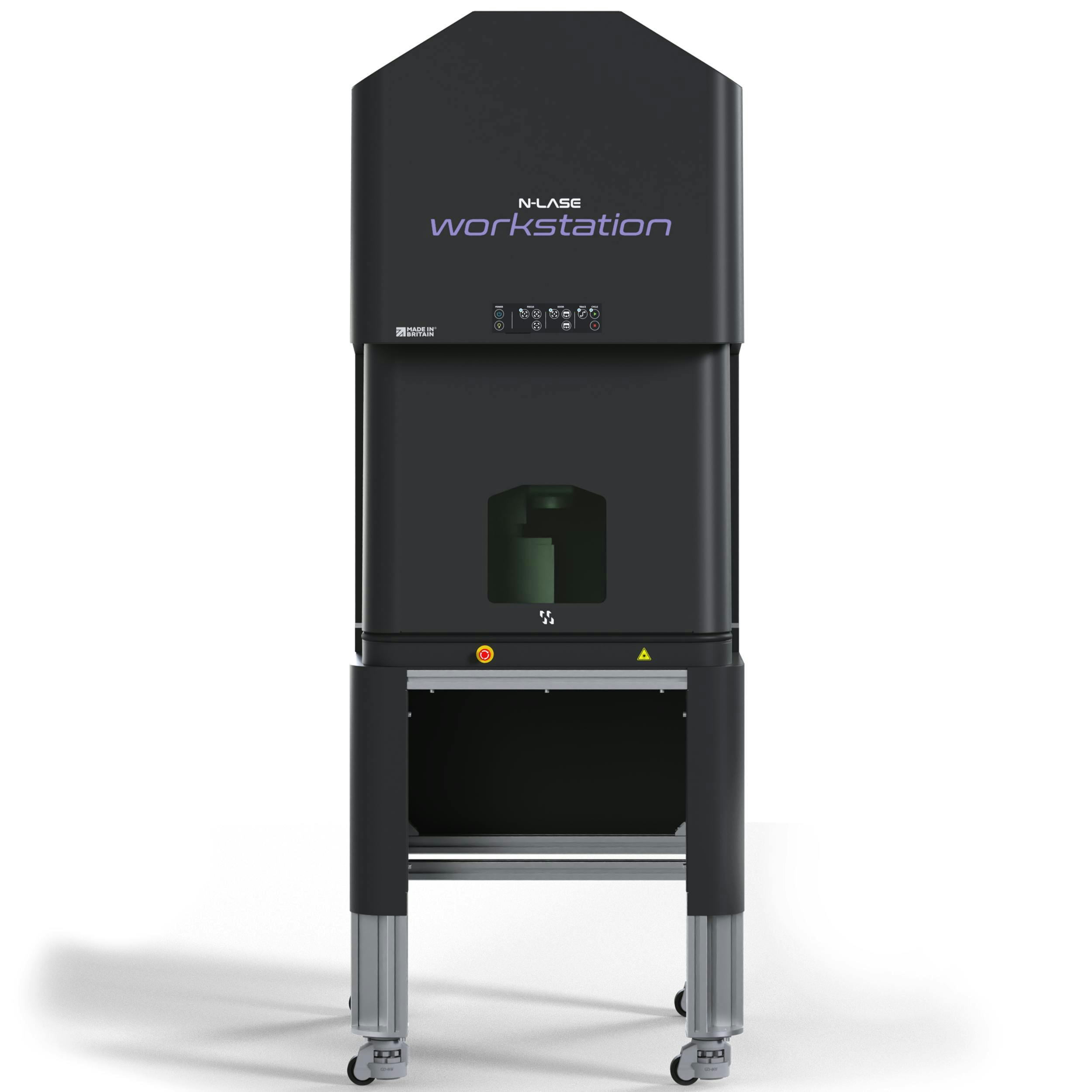
The N-Lase Workstation offers our biggest enclosure mounted onto a portable base to offer maximum flexibility. The Workstation can be located within an existing manufacturing process or operate as a standalone marking and traceability station. With an integrated PC and auto door function, the N-Lase Workstation is a truly turnkey solution; simply wheel into the desired location and start etching.

With such a large enclosure, the N-Lase Workstation can be fitted with a wide range of options to further increase efficiencies and offer maximum throughput. Options include XY marking tables to facilitate the loading of multiple parts, large marking area lenses (up to 280mm x 280mm), big rotary attachments for circumference marking on large diameter parts and power sources from 20 Watt up to 100 Watt for maximum speed and depth.

As with all our N-Lase range, maximum reliability and robustness is assured with our 3-year comprehensive warranty.

N-Lase Integrated

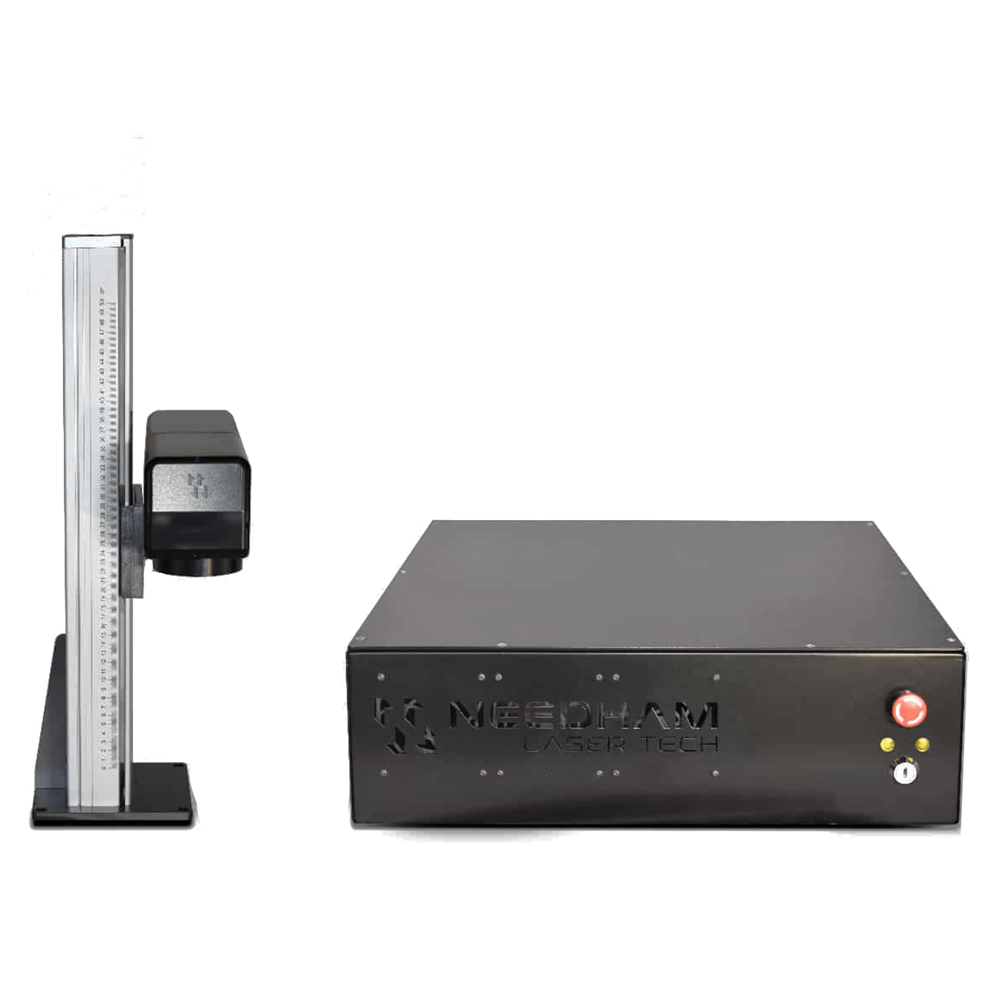
Designed for integration into production, manufacturing and assembly lines, our N-Lase Integrated models offer high reliability, speed and flexibility in a convenient form factor. A wide range of laser power outputs on our standard system allow marking on a diverse variety of substrates, whereas the Integrated Max is suitable for more powerful hungry applications and much larger laser modules. N-Lase Integrated systems are maintenance free and will provide you with years upon years of trouble-free operation

N-Lase Handheld

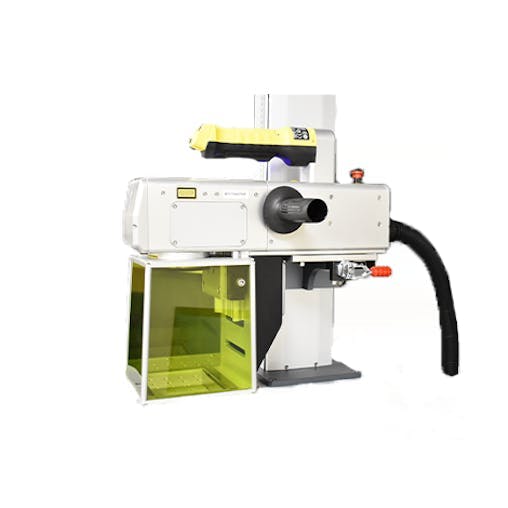
Laser without limits with the N-Lase Handheld. This model allows you to move the system to wherever (and whatever) needs to be marked. Ease and usability is at the forefront of the design, including a counterbalanced laser head to ensure safe movement and use. Whether it's a plaque on a wall or a plate on the floor, this model is ready for the challenge.

Laser Etching PCB and Electronics

Laser etching, or laser marking, refers to the use of lasers to engrave an object. In this process, a highly focused laser is directed onto a specific point or pattern on the object of interest, thereby using the energy from the laser to create very accurate and controlled markings.

Lasers can typically focus on a very small area - about a fraction of a millimetre - while keeping the surrounding area unaffected. The markings are the result of the laser's energy vaporising the material or causing the material to fracture and flake off the surface.

The Benefits of Electronics Laser Marking & PCB Laser Etching Machines

Laser marking is a technology that scales up well in response to increasing demand, while still maintaining efficiency, quality, and safety. It is a quick and fully automated process that can fit right into a production line. Additionally, being a non-contact method of etching or marking, it reduces the wear and tear that the original material goes through during the marking process.

The laser system is also capable of etching highly detailed designs - both accurately and consistently. Dynamic data such as serial numbers and part numbers can be integrated into the process without the need to change parts or for regular user intervention. Most laser etching equipment also comes with software that has been developed to be user-friendly and easy to learn.

Systems Ideal for Laser Marking Electronics

We pride ourselves on only providing the best-in-class electronic laser marking systems, perfectly designed for anything from light use to the most demanding environments:

  • All of our systems feature high-powered MOPA Fiber Laser Engines. Not only does this mean their lifespan is far greater than other lasers on the market but also provides you with a high peak power and extremely quick processing times, and grants maximum application flexibility.
  • Mark text, graphics, barcodes, 2D, UID, Matrix, QR codes and more onto parts with industry-leading accuracy.
  • Incredibly simple setup, programming and marking with great software and ergonomic design.
  • Choose from stand-alone, desktop, benchtop, handheld or integrated laser systems. We will even create custom solutions and can help you implement them into your already automated production line.
  • Brimming with cutting-edge features for the best experience maintaining unparalleled quality while marking your components.

What is a MOPA Fiber Laser?

MOPA fiber lasers are advanced industrial marking tools that offer flexibility, precision, and high-quality performance. They are based on Master Oscillator Power Amplifier (MOPA) configuration, which enables them to generate a wide range of pulse durations and frequencies. This versatility allows them to be used across various materials and industries, including aerospace, automotive, electronics, and medical. Key benefits of MOPA fiber lasers include their high peak power, efficient energy consumption and low maintenance requirements. Find out more about what a MOPA fiber laser is on our blog.

Why Choose Needham Laser Tech for Laser Marking in Electronics?

Laser marking systems are a versatile and cost-efficient solution for the electronic industry, allowing manufacturers to quickly and accurately mark parts with high precision. These systems offer several key benefits compared to traditional methods such as chemical etching or ink-stamping.

First, laser marking systems use lasers to create extremely high-quality marks that are both exact and permanent, meaning they will not fade over time. This makes them ideal for traceability and anti-counterfeiting measures, which is especially important in the electronics industry. Additionally, the marks created by laser marking systems can be used on a wide range of materials including metal, plastic and ceramics. These systems are also very efficient since they have no setup time or cleanup costs associated with them.

Finally, laser marking systems offer greater flexibility since they can quickly switch between different designs while still maintaining quality standards. Furthermore, the accuracy levels of these systems can easily be adjusted depending on the needs of your project - from just above 0.01mm up to 5mm accuracy per design element - ensuring you get exactly the results you need without sacrificing quality.

Needham Laser Tech leads the way when it comes to laser marking system solutions for clients in the electronics industry. Our cutting-edge technology ensures you will get superior results every time! Contact us today to learn more about how our laser marking services can help streamline your production process and maximise your profits.

FAQs About Electronics Laser Marking & PCB Laser Etching Machines

What are the advantages of PCB laser etching?

PCB laser marking machines are considered the best solution for electronics marking for several reasons:

  • High precision: Laser etching allows for extremely precise and accurate patterns and designs, with very tight tolerances. This makes it ideal for applications that require high levels of accuracy and precision.
  • High resolution: Laser etching can produce very fine features and lines, with resolutions down to a few microns. This is particularly useful for the miniaturisation of electronic components.
  • Fast turnaround time: Laser etching can be done quickly and easily, allowing for rapid prototyping and faster time-to-market for new products.
  • Flexibility: Laser etching can be used on a variety of materials, including copper, aluminium, and even ceramic substrates. This makes it a versatile and flexible process for PCB fabrication.
  • Minimal waste: Unlike traditional PCB fabrication methods, laser etching produces very little waste material, resulting in a more environmentally-friendly process.
  • No physical contact: Laser etching is a non-contact process, which means there is no physical contact between the etch tool and the workpiece. This reduces the risk of damage to the PCB and ensures a longer tool life.

Overall, PCB laser etching offers many advantages over traditional methods of PCB fabrication, making it a popular choice for prototyping and small-scale production of electronic components. Our laser systems offer the highest standard of each of the benefits outlined above, allowing businesses to grow alongside the industry's ever-changing standards, regulations and customer demands.

How does PCB laser etching work?

PCBs are the backbone of modern electronics, with their layers of conductive pathways forming intricate circuits to power our everyday devices. As such, these boards must be highly precise and accurate to ensure optimal performance - this is where PCB laser etching comes into play.

Simply put, PCB laser etching is a process that uses laser technology to create the desired electrical pathways onto a PCB by removing copper-clad material from the specified areas without damaging other components. In contrast to traditional methods, such as mechanical drilling and chemical etching, laser etching offers much more accuracy and control over the desired results, making it ideal for sophisticated circuitry designs.

The process starts with creating a CAD file of the desired circuitry layout, which ensures that all instructions regarding the printed circuit board design are precisely followed during the entire etching process. This design is then sent to a laser-etching machine that is fitted with at least two laser settings and one high-power laser head; typically YAG lasers (Yttrium Aluminium Garnet) are used due to their accuracy and minuscule heat-affected zone produced in comparison to CO2 lasers.

Once all instructions have been inputted, the machine will then scan each layer in turn before focusing its powerful laser beam on areas designated for removal - vaporising or ablating away material until all desired markings have been produced onto the board. The amount of energy required for each layer varies depending on its properties but generally speaking, shallow cut depths can be achieved quickly and accurately using this method.

Overall, when considering both speed and precision, PCB laser etching provides manufacturers with an efficient way of producing complex and accurate circuitry in shorter production cycles than ever before.

What materials can be used for PCB laser etching?

PCB laser etching can be achieved with a range of materials, including copper, stainless steel, aluminium, titanium, tin-plated copper and glass epoxy. The choice of material depends on the required performance characteristics for the finished product. 

Aluminium is a commonly used material for PCB laser etching as it offers excellent heat dissipation and light reflection properties. 

Brass is a popular material for PCBs due to its excellent electrical conductivity, durability, and corrosion resistance. Laser marking is an ideal solution for marking brass PCBs because of its ability to create high-quality, precise markings with excellent contrast and legibility.

Cast iron is commonly used in electronic applications due to its high strength and durability.

Copper is the most common material used for PCB laser etching due to its high melting point and durability.

Gold is an important element in the design of PCBs, and laser marking delivers a highly-detailed visible marking that is resistant to fading. The non-contact application of laser marking makes our products an excellent solution. 

Metals such as brass, copper, aluminium, and stainless steel are commonly used in PCBs due to their excellent electrical conductivity and durability.

Plastics such as polycarbonate, polyamide, and polyethylene are frequently used in PCBs due to their durability, heat resistance, and electrical insulation properties.

Rubber is commonly used in PCBs for its insulation and sealing properties.

Sterling silver is sometimes used in PCBs for its electrical conductivity and corrosion resistance.

Wood is not typically used as a material in PCBs due to its poor electrical conductivity. However, laser marking is a popular method for marking wooden enclosures or other wooden parts used in electronic products as it is a safer, non-contact method of application.

What is the resolution of laser etching for PCBs?

The resolution of laser etching for PCBs is usually determined by the type and power of the laser used. A low-power laser, such as a diode laser, offers resolutions as low as 15 µm (micrometres). Higher-powered lasers, such as CO2 lasers, can achieve resolutions up to 50 µm or higher. The resolution of the laser also depends on the material being etched; copper and aluminium materials offer the best results in terms of resolution.
How can I design a PCB layout for laser etching?

To design a PCB layout for laser etching, it is important to consider the type of laser being used and the desired resolution. It is also important to include sufficient spacing between components and traces, as well as ensure that all patterns are properly sized. To ensure an accurate laser etching process, it is recommended to use a professional CAD software such as Altium Designer or AutoCAD. Additionally, careful consideration should be given to the design rules that define things like trace widths and clearances in order to achieve optimal results.

Contact us Today

Any business in the electronics industry faces the challenge of high-quality, precise marking at a large volume with no compromise on output. Find out how Needham Laser Tech can help you integrate laser marking systems into your manufacturing or production line today by contacting our specialist team, either by phone on 01948 660 011 or by filling out our contact form.

60+ years in industry

Heritage & market-leading knowledge

The Needham Group and its subsidiaries have been a part of the ever-developing coding and marking industry since 1962; identifying industry needs whilst simultaneously importing and developing exciting, practical and innovative products to suit.

Community-driven

Customer service at our core

Every day we share our passion and excitement for British manufacturing and innovation in laser technologies with each of our partners; from supplier and supply chain right through to end-user.

Short lead times

Delivery in weeks, not months

We design, develop and manufacture our lasers at our HQ in Shropshire; allowing for lean manufacturing, better efficiencies and speedy response times in our manufacturing, ultimately getting your products to you in weeks rather than months.

Made in Britain & Safety Regulations

We are proud to wear the Made in Britain badge, where all of our lasers are manufactured at our HQ in Shropshire. Combining over 60 years of company heritage with exquisite design and Great British engineering, we take great pride in our heritage and our commitment to producing quality products that represent the very best of British craftsmanship. Our loyal customers can be assured that when they choose us, they are investing in a product made with the utmost care and attention to detail.

The UK has the world's most rigorous regulatory requirements for laser safety.
We are proud to align our UK design and manufacturing with said regulations.
We are also certified members of AILU. - https://www.ailu.org.uk/

Trusted By The Best

Enquire Now